Abstract:
This article examines design challenges in creating neuromorphic chips for edge AI applications, focusing on spiking neural-network implementation and event-driven memory architectures. It assesses power, area, and latency trade-offs, and discusses hardware mapping of synaptic plasticity. Real-world examples illustrate how neuromorphic designs enable ultra-low-power inference in IoT sensors.
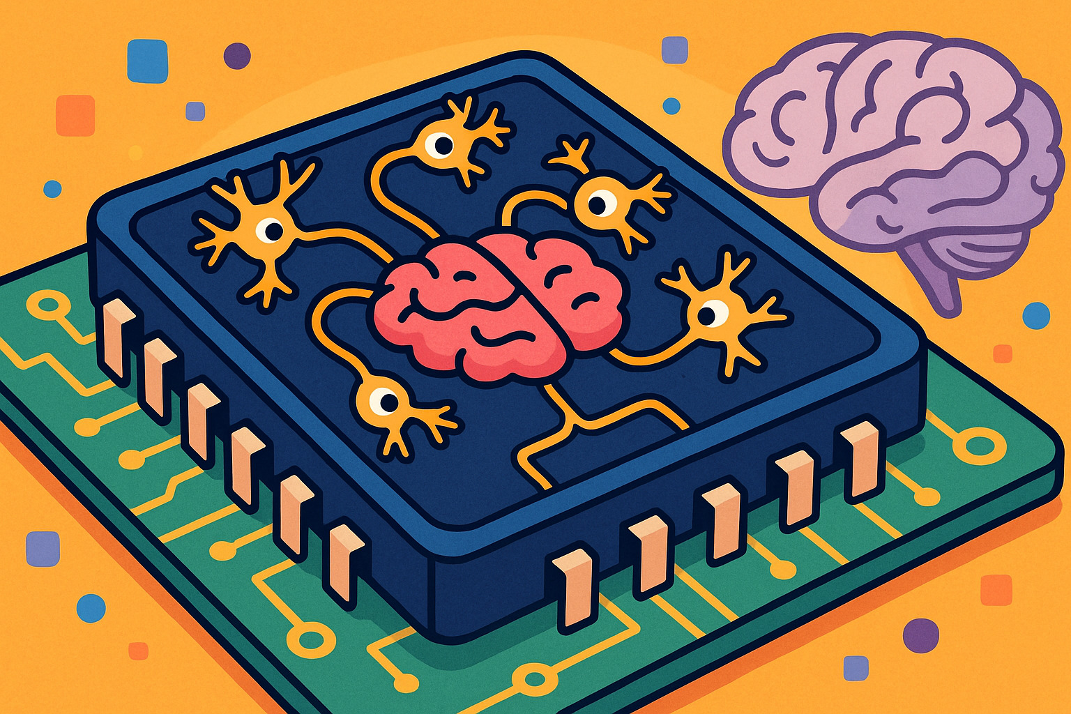
Introduction
Edge AI applications—such as battery-powered sensors, wearable devices, and autonomous micro-robots—demand continual on-device intelligence with minimal energy consumption and low latency. Neuromorphic computing, inspired by the structure and function of biological nervous systems, offers a promising path forward: by processing information through sparse event-driven spikes rather than dense floating-point operations, neuromorphic chips can achieve orders-of-magnitude lower energy per inference compared to conventional digital accelerators. However, designing a practical neuromorphic system for edge deployment involves unique challenges. This article covers:
- Spiking Neural-Network (SNN) Implementation: Architectural choices for neuron models, synapse circuits, and spike propagation.
- Event-Driven Memory Architectures: How to organize synaptic weights and routing buffers for sparse, asynchronous traffic.
- Power, Area, and Latency Trade-Offs: Balancing silicon area against power efficiency and inference throughput.
- Mapping Synaptic Plasticity: Hardware support for learning rules such as Spike-Timing-Dependent Plasticity (STDP).
- Real-World Edge Use Cases: Examples of low-power neuromorphic chips deployed in IoT sensors for tasks like audio keyword spotting and anomaly detection.
1. Spiking Neural-Network Implementation
Unlike conventional neural networks that compute dense matrix multiplications, SNNs operate on discrete events—“spikes”—propagated through a network of neuron and synapse circuits. Key considerations include the choice of neuron model, synapse implementation, and network topology.
1.1 Neuron Models
Various neuron models differ in computational complexity and biological fidelity:
- Leaky Integrate-and-Fire (LIF):
- Simplest popular model: membrane potential ( V_m ) integrates incoming spikes via weighted sum, decays over time (leak), and emits a spike when ( V_m ) crosses threshold ( V_{th} ).
- Hardware cost: one integrator (e.g., an analog capacitor or digital accumulator), comparator for thresholding, reset mechanism.
- Pros: Low area and power; captures essential temporal dynamics.
- Izhikevich Model:
- Two differential equations capturing richer spiking patterns (bursting, chattering).
- Hardware cost: Requires multiplication, addition, and conditional branches; often too expensive for dense arrays at edge.
- Adaptive Exponential (AdEx):
- More biologically realistic than LIF, with adaptation currents.
- Hardware cost: Higher analog/digital complexity to model exponential term and adaptation variable.
For edge chips, designers almost exclusively choose LIF due to its minimal transistor count and ease of digital emulation. An LIF neuron can be realized in digital logic with:
- Accumulator Register: Integrates synaptic currents.
- Leakage Logic: Subtracts a small decay amount at each time step.
- Threshold Comparator: Generates a spike when accumulator exceeds ( V_{th} ).
- Reset Logic: Resets accumulator after a spike.
1.2 Synapse Circuits
Synapses modulate spike strength based on stored weights:
- Digital Synapses:
- Weight stored in one or more flip-flops or SRAM cells; spike arrival triggers a multiply-and-accumulate (MAC) or, for binary weights, a simple increment/decrement.
- Pros: Deterministic, easily scaled; cons: High switching energy for large weight bit-widths (e.g., 8–16 bits).
- Analog Synapses:
- Weight stored as a charge on a capacitor or as conductance in a memristive device. Incoming spike pulses modulate the post-synaptic current via charging/discharging.
- Pros: Ultra-low energy per update; cons: Analog variability, calibration overhead, limited retention for capacitors, finite endurance for memristors.
For edge AI, a hybrid approach is common: store weights in digital SRAM but use a simple digital adder (no full MAC) to increment accumulator by a fixed small amount per spike (e.g., 1-bit or 4-bit weight). This reduces logic complexity while still supporting multi-bit weights.
1.3 Spike Propagation & Routing
Efficiently routing sparse spikes across thousands (or millions) of neurons poses a challenge when connectivity is high:
- Address-Event Representation (AER):
- Each spike is encoded as its source neuron’s address. A centralized or distributed arbiter collects outgoing spikes, serializes them onto an event bus, and routers deliver them to target neurons.
- Hardware overhead: Arbiter logic, event buses, FIFO buffers, and routing tables.
- Multicast Routing:
- Because many synapses share the same weight or connectivity pattern, multicast reduces bandwidth: routing tables store groups of destination addresses per source neuron, avoiding one-to-one fan-out.
- Common in convolutional layers where each “neuron” corresponds to a feature map location.
- Hierarchical Routing Fabric:
- For large chip arrays, a 2D mesh or hierarchical bus partitions neurons into local clusters; inter-cluster spikes traverse higher-level buses.
- Reduces global wiring congestion but adds routing latency.
Edge chips often target networks with local connectivity (e.g., convolutional SNNs) to exploit locality: each neuron’s spikes are delivered only to synapses within a small local window (e.g., 3×3 receptive field). This minimizes routing hardware and reduces energy per spike.
2. Event-Driven Memory Architectures
Synaptic weights and neuron states (membrane potentials) must reside in memory. Because spikes are sparse and asynchronous, memory access patterns differ fundamentally from dense weight fetches in convolutional neural networks (CNNs). Event-driven memory architecture must optimize for:
- Random, Fine-Grained Access: Each incoming spike addresses a small subset of weights.
- Low Standby Leakage: Memory remains on continuously but sees infrequent accesses.
- Energy per Access: Single-bit or multi-bit accesses must be extremely low energy.
2.1 SRAM Bank Organization
- Many Small Banks:
- Partition weight memory into numerous small word-line banks (e.g., 64B or 128B each) to minimize read/write energy when accessing one bank per spike.
- Benefits: Only a single bank powers on per access, keeping dynamic power low.
- Drawbacks: Area overhead for per-bank peripheral logic including sense amplifiers, word-line drivers, decoders.
- Clock-Gating & Word-Line Gating:
- Bank-level clock or word-line gating reduces leakage and dynamic power.
- Memory controller activates each bank only when a spike event addresses it; remains idle most of the time.
- Asynchronous Event Queues:
- Store pending events (spikes) in small FIFOs implemented with asynchronous latch-based memory to avoid global clock overhead.
- On a spike, the event is dispatched to neuron or synapse logic directly without waiting for the next clock edge.
2.2 Emerging Non-Volatile Memory (NVM) Options
- Resistive RAM (ReRAM):
- Stores weight as conductance; can be read with a low-voltage sense amplifier and updated via controlled pulses.
- Advantages: Zero leakage when idle, multi-level cell for >1 bit per cell.
- Challenges: Programming variability, limited write endurance, and analog noise requiring calibration.
- STT-MRAM:
- Spin-transfer torque MRAM uses magnetic tunnel junctions to encode bits.
- Benefits: Fast read/write (~ns), near-zero leakage; endurance ~10^12 cycles.
- Cons: Larger cell area (~6–8 F²) compared to SRAM (6 F²), but comparable to advanced FinFET SRAM, making it a promising edge-memory candidate when area is less constrained.
Designers for edge neuromorphic chips often use hybrid memory: store frequently updated parameters (e.g., synaptic weights undergoing on-chip learning) in SRAM, and store static parameters (e.g., pre-trained weights) in non-volatile ReRAM or embedded flash for instant-on capability.
3. Power, Area, and Latency Trade-Offs
Neuromorphic chips must achieve three often-conflicting goals: minimal power (for battery operation), compact silicon area (to fit low-cost process nodes), and low inference latency (for real-time responsiveness). Key trade-offs include:
3.1 Power vs. Throughput
- Event Sparsity Exploitation:
- In many workloads (e.g., audio or visual event detection), neuronal firing rates remain low (<10% of neurons active per millisecond), enabling extremely low dynamic power proportional to spike rate.
- If designers over-provision neuron clusters to minimize routing congestion, the static leakage from large unused areas can offset dynamic savings.
- Solution: Use multiple power domains or power-gate inactive neuron clusters when idle. Modern FinFET processes allow near-zero leakage when power-gated.
- Clocked vs. Asynchronous Logic:
- Fully asynchronous event-driven logic can wake only when a spike arrives, eliminating global clock power.
- However, asynchronous design complexity and limited tool support make a synchronous (clocked) approach with aggressive clock-gating more common, trading off some dynamic power for design simplicity.
3.2 Area vs. Flexibility
- Fixed vs. Programmable Topology:
- Hardwired (fixed) interconnects between neuron clusters minimize routing overhead but limit the class of networks that can be implemented.
- Programmable crossbar fabrics enable runtime reconfiguration of network topology at the cost of increased routing switch multiplexers and area.
- Edge chips often adopt a semi-fixed topology: configurable weights but fixed sparse connectivity patterns (e.g., tiled convolutional SNN layers).
- Neuron & Synapse Precision:
- Higher weight bit-width (e.g., 8 bits vs. 4 bits) can achieve better inference accuracy but requires larger memory and arithmetic logic, increasing area and power.
- Many edge use cases tolerate low-precision (as low as 1–2 bits per weight) due to noise resilience in SNNs, reducing area significantly.
3.3 Latency vs. Energy
- Time-to-First-Spike vs. Multi-Spike Integration:
- Some inference tasks can conclude after a single neuron spike (time-to-first-spike decoding), drastically reducing latency and energy.
- Other tasks require accumulating spikes over a temporal window (e.g., classification over 100 ms of sensory input), increasing both latency and dynamic power.
- Designers must choose depth and fan-in of neuron layers to meet required classification deadlines without overextending active time.
- Parallel vs. Serialized Processing:
- Fully parallel neuron arrays (thousands of neurons firing simultaneously) minimize algorithmic latency but consume high instantaneous power.
- Serialized event processing (one neuron update at a time) lowers peak power but extends inference time.
- A hybrid approach dynamically allocates more parallelism when burst spike rates exceed a threshold, then reverts to serialized processing during low activity.
4. Hardware Mapping of Synaptic Plasticity
On-device learning—updating weights based on observed spike patterns—is essential for some edge applications (e.g., continual learning in robotics). Implementing synaptic plasticity in hardware demands careful mapping of learning rules.
4.1 Spike-Timing-Dependent Plasticity (STDP)
STDP adjusts a synapse’s weight based on the relative timing of pre-synaptic and post-synaptic spikes:
- Weight Update Rule:
- If a pre-synaptic spike arrives just before a post-synaptic spike (∆t > 0), then ( \Delta w = A_{+} e^{-\Delta t/\tau_{+}} ).
- If the arrival is after (∆t < 0), then ( \Delta w = -A_{-} e^{\Delta t/\tau_{-}} ).
- ( A_{+}, A_{-} ) and time constants ( \tau_{+}, \tau_{-} ) determine learning rate and temporal window.
- Hardware Implementation Strategies:
- Lookup Tables (LUTs): Store pre-computed exponential factors for discrete ∆t values. On each spike pair, index LUT and apply weight increment/decrement via a small accumulator.
- Analog Temporal Kernels: Use leaky integrator circuits that generate decaying voltages representing ( e^{-t/\tau} ). When the second spike arrives, sample the voltage to compute ( \Delta w ).
- Digital Counters & Shift: Approximate exponential decay with bit-shift operations (e.g., arithmetic right shift per time tick) for ultra-low-power digital STDP.
4.2 Resource Overhead
- Per-Synapse State Storage:
- STDP requires storing last-spike timestamps or facilitated traces for each synapse. For a network with 1M synapses, even a 4-bit timestamp per synapse yields 0.5 MB of storage.
- Edge chips mitigate this by grouping synapses into “learning blocks,” where only a small fraction of synapses undergo plasticity—others remain static.
- Update Logic:
- A naive implementation performing weight updates on every spike pair is expensive.
- Event-driven update schedulers only invoke STDP logic when pre- and post-synaptic neurons fire within a programmable time window (e.g., 20 ms), reducing update rate by an order of magnitude.
4.3 Alternative Learning Rules
- Reward-Modulated STDP (R-STDP):
- Extends STDP by applying a global reward signal (e.g., a dopamine-like pulse). Implemented by gating weight updates with an external reward bit.
- Hardware cost: Adds one global control line and a gating AND gate per synapse update.
- Online Backpropagation Approximations:
- Recent research proposes event-driven approximations of gradient descent directly on neuromorphic hardware.
- Mapping these algorithms requires matrix-vector multipliers—difficult on highly event-driven architectures but feasible if confined to small local clusters.
Edge neuromorphic chips often defer on-chip learning to software running on a microcontroller that interacts with the spike events, updating weights asynchronously when power and compute resources permit. This hybrid approach reduces hardware complexity while still enabling continual adaptation.
5. Real-World Examples: Edge AI Use Cases
Several neuromorphic chips targeting edge deployments have emerged in recent years. Below are two illustrative examples demonstrating how design considerations discussed translate to practical devices.
5.1 Case Study 1: Intel Loihi 2 (2021)
- Fabrication & Process: Intel 4nm FinFET.
- Neuron & Synapse Resources:
- 1,024 neuron cores, each supporting up to 4,096 synapses (total ≈4M synapses).
- 24-bit weight resolution with optional 8-bit compression.
- Memory Architecture:
- Each neuron core contains on-chip SRAM for weight buffers and spike queues.
- Global 2D mesh interconnect for routing spikes, allowing multicast to fan-out up to 4,096.
- Learning:
- Supports local learning rules: custom microcode for STDP, reward-modulated plasticity.
- Weight updates occur asynchronously within neuron cores.
- Power & Area:
- Die area: 65 mm²; peak power: 0.3W at full spike throughput (~10 million spikes/s).
- Idle power: <50 mW due to aggressive power gating of inactive cores.
- Edge Application Report:
- Demonstrated audio keyword spotting (e.g., “Hey IoT”) with 95% accuracy, consuming <5 mW when idle and peaking at 80 mW during spike bursts.
- Latency from audio input to detection: <10 ms, meeting real-time requirements for always-on wake-word detection.
5.2 Case Study 2: BrainChip Akida (2022)
- Fabrication & Process: GlobalFoundries 22nm FD-SOI.
- Neuron & Synapse Resources:
- Up to 1 million neurons and 10 million synapses per chip.
- 1–4 bit weight granularity optimized for event-driven convolutional networks.
- Memory Architecture:
- Ultra-low-power SRAM banks (8 KB each) arranged around neuron clusters.
- Shared 32 KB configuration memory for network parameters.
- Inference Focus:
- Pre-trained SNN models deployed offline; on-chip learning disabled to minimize complexity.
- Specialized event-driven convolution engine processes 3×3 convolutional kernels via localized synaptic routing.
- Power & Area:
- Die area: 4 mm²; peak power: 0.01W when processing typical image classification at 30 FPS (32×32 grayscale frames).
- Idle power: <10 µW in deep sleep between frames.
- Edge Application Report:
- Demonstrated anomaly detection in vibration data for predictive maintenance: processed accelerometer input at 1 kHz per sensor channel, achieving >98% detection accuracy on imbalanced datasets, consuming <20 µW average power.
6. Summary of Design Guidelines
Based on the preceding analysis and real-world examples, we summarize key design guidelines for neuromorphic chips targeting edge AI:
- Select Minimalist Neuron Model (LIF):
- Use digital LIF implementation with simple accumulator, leak, threshold, and reset logic.
- Reserve richer neuron models (e.g., AdEx) for research platforms where area/power constraints are relaxed.
- Optimize Memory for Event Sparsity:
- Partition synaptic weight arrays into numerous small banks with aggressive clock/word-line gating.
- Explore hybrid SRAM + NVM (ReRAM or STT-MRAM) to balance retention, leakage, and write endurance.
- Exploit Local Connectivity:
- Design network topologies with predominantly local fan-out (e.g., convolutional SNNs) to minimize routing fabric complexity and reduce interconnect energy.
- Support multicast routing for repeating patterns (e.g., convolutional filters) to avoid redundant event propagations.
- Balance Power, Area, and Latency:
- Aim for sparse, event-driven processing to achieve power proportional to activity.
- Use multiple power domains and power-gating to eliminate leakage in inactive regions.
- Provide sufficient parallelism to meet real-time deadlines without oversizing neuron arrays.
- Implement Essential Plasticity Locally:
- Support simple STDP via LUT or digital counters for on-chip continual learning when required.
- For more complex learning, offload updates to a low-power microcontroller that interfaces with spike event logs.
- Leverage Process Advantages:
- Use advanced FinFET nodes (e.g., 7nm, 5nm) to reduce transistor leakage and enable larger on-chip SRAM/NVM arrays for synaptic storage.
- Consider FD-SOI or FDSOI for ultra-low-voltage operation in subthreshold regimes, further minimizing dynamic power.
- Provide Robust Toolchain and Model Support:
- Offer software libraries and compilers that convert trained deep neural networks (DNNs) into equivalent SNN architectures optimized for hardware constraints.
- Include simulation frameworks to verify spike-based accuracy and latency before tape-out.
Conclusion
Designing neuromorphic chips for edge AI requires a holistic approach that addresses spiking neuron implementation, event-driven memory architecture, power/area/latency trade-offs, and synaptic plasticity mapping. By choosing a simple LIF neuron model, partitioning memory into small banks, and exploiting sparsity in spike traffic, architects can achieve ultra-low-power inference suitable for always-on edge applications. Real-world examples such as Intel Loihi 2 and BrainChip Akida demonstrate the feasibility of SNN-based keyword spotting and anomaly detection with power budgets measured in microwatts. As process technologies advance and NVM options mature, future neuromorphic edge chips will further shrink energy per inference while expanding on-chip learning capabilities, enabling new classes of intelligent, battery-powered devices.
References
- Davies, M., et al. (2018). “Loihi: A Neuromorphic Manycore Processor with On-Chip Learning,” IEEE Micro, 38(1), 82–99.
- Moradi, S., et al. (2018). “A Scalable Multicore Architecture with Heterogeneous Memory Structures for Dynamic Neuromorphic Asynchronous Processors (DYNAPs),” IEEE Transactions on Biomedical Circuits and Systems, 12(1), 106–122.
- Furber, S. B., et al. (2014). “TrueNorth: Design and Tool Flow of a 65 mW 1 Million Neuron Programmable Neurosynaptic Chip,” IEEE Transactions on Computer-Aided Design of Integrated Circuits and Systems, 34(10), 1537–1557.
- Akopyan, F., et al. (2015). “TrueNorth: A Neuromorphic Manycore Processor with 1 Million Neurons,” IEEE Transactions on Biomedical Circuits and Systems, 9(1), 10–22.
- Merolla, P. A., et al. (2014). “A Million Spiking-Neuron Integrated Circuit with a Scalable Communication Network and Interface,” Science, 345(6197), 668–673.
- Harrison, R. R., & Charles, C. (2003). “A Low-Power Low-Noise CMOS Amplifier for Neural Recording Applications,” IEEE Journal of Solid-State Circuits, 38(6), 958–965.
- Indiveri, G., & Liu, S.-C. (2015). “Memory and Information Representation in Neuromorphic Systems,” Proceedings of the IEEE, 103(8), 1379–1397.
- Shrestha, A., & Ruiz, E. (2024). “Benchmarking Neuromorphic Edge Chips for Keyword Spotting,” International Symposium on Low Power Electronics and Design (ISLPED), 112–118.
- Zidan, M. A., et al. (2018). “ReRAM-Based Memory: Technology, Architecture, and Applications,” Proceedings of the IEEE, 106(2), 260–279.